'Basics of Traveling Wave Tubes Amplifiers'
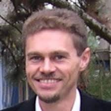
Frédéric Andre, Product Line Architect at Thales AVS, Vélizy-Villacoublay, France
Tuesday, April 27, 2021
09:00 - 10:30 AM
Abstract
Traveling Wave Tubes enable high performance amplification systems with very high efficiency and data rate. In this mini-course we explain how this wonderful device works. We emphasize on helix pitch tapering and multi stage depressed collector techniques which are key for high power efficiency.
Biography
Mr. Frédéric André is presently acting as product line architect at Thales AVS. He develops traveling wave tubes for space applications in Vélizy-Villacoublay (France) and Ulm (Germany). His interests extend to advanced concepts including Hamiltonian time domain model of TWTs, carbon nanotube cathodes, and sub-terahertz TWTs.
__________________________________________________________________________________________________________________________________
'Satellite radio-frequency payloads and instruments - Overview and challenges'
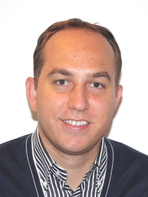
Salvatore D’Addio, Head of Payload Engineering Section, RF Payloads & Technology Division, Electrical Department,
Directorate of Tech, Eng. & Quality, European Space Agency, ESTEC, Noordwijk, The Netherlands
Tuesday, April 27, 2021
10:50 - 12:20 AM
Abstract
Overview and future trends of architectures, key technology requirements and driving design aspects for:
Biography
Salvatore D'Addio received a Telecommunication Engineering master degree from the University of Naples in 2005 and ra master degree in Satellite Systems from the University of Rome in 2006.
He received a PhD in Electronics and Telecommunications Engineering from University of Benevento in 2017.
Since 2004 he worked on design and development of optoelectronics sensors at the University of Benevento and on RF characterization and testing of 3G mobile terminals at H3G, Rome.
In 2006 he joined the European Space Agency as RF payload engineer covering sveral R&D activities and projects support on modelling, analysis, design and development of telecommunication payloads and microwave remote sensing instruments.
Since 2013 he has covered the position of principal instrument engineer of the Microwave Imager radiometer (MWI) in the MetOp-SG satellite meteorological program, managing technology pre-developments and the overall Phase B2/C/D activities for instrument design, development and testing.
Since 2018, Salvatore D'Addio is Head of the Payload Engineering Section within the RF Payloads and Technology Division at the European Space Agency. His interests cover the research, design, development and testing of telecommunication payloads and sub-systems, microwave and millimetre wave remote sensing instruments and navigation
payloads exploiting analogue, digital and optical on-board technologies.
__________________________________________________________________________________________________________________________________
'Additively Manufactured RF parts - what, why, when, where, who and how'

Petronilo Martin-Iglesias, EO Microwave Payload Engineer in the Microwave Instruments Section, Future Missions &
Instruments Division, Future Systems Department, Directorate of EO, European Space Agency, ESTEC, Noordwijk, The Netherlands
Tuesday, April 27, 2021
12:40 - 2:10 PM
Abstract
At this moment in time everyone has heard about additive manufacturing to build 3D structures. Material and processes engineers are working hard to develop new process and extend the range of materials which can be used for the manufacturing. An impressive range of materials is already available as a response to demands from different applications going from medicine to automotive but also for space applications. RF engineers are, for sure, welcoming the new materials and processes a new variable to be considered during the design to enhance further the performance. This ecosystem is excellent but, considering the number of options, the selection of the end-to-end product cycle (from definition to characterization) has to be carefully performed to check if, the use of advanced manufacturing techniques is justified. This presentation introduces the main aspects to be addressed when additive manufacturing is considered for a space product. WHAT are the components/sub-systems than can benefit from these techniques, WHY do we want to use AM, WHEN is justified to use AM instead of more conventional manufacturing ways, WHERE the improvement can be achieved, WHO should be involved in the product development and HOW the process has to be introduce in the end to end process.
Biography
Petronilo Martín-Iglesias (M’12) was born in Caceres, Spain, on April 23, 1980. He received the Telecommunication Engineering degree from the Polytechnic University of Madrid, Madrid, Spain, in 2002, and the Master degree from The University of Leeds, Leeds, U.K., in 2012.
He has been working in industry for over ten years as a Microwave Engineer involved with active (high power amplifiers for radar applications) and passive (filters, multiplexers, couplers, etc.) RF hardware design, including two years as a Radar System Engineer with Indra Sistemas, ISDEFE S.A., and Thales Alenia Space Spain. Since Summer 2012, he has been involved with research and development and project support activities related with RF passive hardware developments for the European Space Agency. His research interests are filter synthesis theory, electromagnetic (EM) design and high power prediction, as well as advanced manufacturing techniques for RF passive hardware. From January 2020 he is part of the Microwave Instruments Section at ESA-ESEC.
__________________________________________________________________________________________________________________________________
'Cathode Emission Mechanisms and Characteristics'

Joan E. Yater, Naval Research Labs, USA
Tuesday, April 27, 2021
3:30 - 5:00 PM
Abstract
This lecture will present an overview of the emission physics and characteristics of thermionic cathodes, secondary (and photo) emitters, and field emitters used in vacuum electronic device technology. Because of the different emission mechanisms associated with these cathodes, the lecture will be broken into three sections that provide the necessary technical background for each cathode area. Each section will then examine the emission characteristics of the cathode as a function of the material properties and operating conditions and will review the challenges and opportunities for improved cathode technology.
Biography
Joan Yater received the A.B. degree in physics from Cornell University in 1982 and the Ph.D. degree in physics from the University of Texas at Austin in 1992. In 1993, she joined the Naval Research Laboratory in Washington, DC as a National Research Council postdoctoral fellow, and in 1995 she became a Research Physicist in the Electronics Science and Technology Division. In her research, she has used her background in surface science and electron spectroscopy to study the electron emission properties of electron sources for vacuum electronic device applications. Her research areas have included secondary emission, photoemission, and thermionic emission, and her studies have particularly focused on wide bandgap materials for cold emission and current amplification applications. She is a member of the American Physical Society and Materials Research Society, and she serves on the International Steering Committee of the International Vacuum Electron Sources Conference.
__________________________________________________________________________________________________________________________________
'Introduction to vacuum electronics at nano-scale for space applications'

Jin-Woo Han, Research Scientist at USRA/NASA Ames Research Center, USA
Tuesday, April 27, 2021
5:20 - 6:50 PM
Abstract
Long-term operation in harsh environment becomes increasingly less sustainable due to several device aging mechanisms. Total ionizing dose (TID) and displacement damage (DD) degradation limit new class of missions including long term (> 20 years) deep-space exploration, nano-spacecraft, Europa mission, and so on. In order to tackle such challenges, in this tutorial, a nanometer scale vacuum channel transistor that combines the advantages of both vacuum and solid-state electronics is provided. The fabricated vacuum channel transistor is introduced and the radiation immunity is experimentally assessed. Incident radiation needs to traverse some distance in the channel to release its energy and liberate electrons from the semiconductor for device degradation to occur. Therefore, the only approach to completely avoid the radiation effects is to utilize a vacuum channel. Unfortunately, as long as the electron emitter and collector structures exist, the vacuum transistor faces mechanical reliability issue associated with the electrode material rupture and degradation in the long term. Our latest results on silicon based nanoscale vacuum channel transistor suggest them to be a robust alternative to silicon based vacuum devices.
Biography
Jin-Woo Han is a Senior Research Scientist at the Center for Nanotechnology, NASA Ames Research Center, Moffett Field, California, USA. He currently leads a research team composed of USRA personnel responsible for developing nanoscale vacuum transistor for next generation nanoelectronics and printed
electronics. He has received the NASA Ames Honor Award, the IEEE Electron Device Society Early Career Award, Outstanding Engineering Achievement Merit Award from Engineers’ Council, the 2015 Mike Sargeant Award from the Institute of Engineering and Technology, IET, UK), IEEE Nanotechnology
Council Early Career Award and the Presidential Early Career Award for Scientists and Engineers (PECASE) Award in 2016. He has published over 100 articles in peer-reviewed journals and given numerous invited talks on his subject areas in national and international conferences and universities.
__________________________________________________________________________________________________________________________________
'Advanced manufacturing for millimeter wave and near-terahertz vacuum electronics'
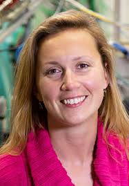
Diana Gamzina, Materials and Manufacturing for MillimetreWave and Near-TherahertzSystems, SLAC National Accelerator Laboratury,
University of California, European Space Agency, Davis, USA
Tuesday, April 27, 2021
7:10 - 8:40 PM
Abstract
The numerous and diverse spectrum of applications have long necessitated the development of vacuum electronic devices (VEDs) that operate in the millimeter and near-terahertz regions. VEDs that operate at these frequencies have structures on the order of a few hundred microns, tolerances of a few microns or less, and surface roughness constraint limits less than an RF skin depth (few tens to few hundreds of nanometers). High frequency VEDs have been enabled by advancements in manufacturing techniques that not only address precision of fabrication, but also produce excellent surface finishes. Some of the proven techniques include LIGA as well as Micro- and Nano-CNC machining. Copper additive manufacturing technology has advanced significantly over the recent years to become a potential solution for fabrication of future VEDs as well. Furthermore, progress in micro and nano scale materials manufacturing of electron sources have enabled generation of high current density electron beams. While vacuum electronics industry remains conservative in their approaches to manufacturing of VEDs, many advancements have been introduced and demonstrated in laboratory environment that will enable wide-spread use of millimeter and near-THz devices.
Biography
Dr. Diana Gamzina joined the SLAC National Accelerator Laboratory in 2017 as a staff scientist. Her interests include mechanics of materials' interaction with electromagnetic waves, micro to nano scale, as well as additive material synthesis techniques, and development of miniature high-frequency RF sources.
__________________________________________________________________________________________________________________________________
'Brazing Science and Engineering for Vacuum Electron Devices'

Scott Forrest, Sr. Engineer at CPI and Co-owner, Altair Technologies, inc, University of California, Barkley, USA
Tuesday, April 27, 2021
9:00 - 10:55 PM
Abstract
Brazing is of great importance for the manufacture of Vacuum Electron Devices. It is the single most important joining technique due to its immense flexibility and versatility. However, it is also the largest cause of failures. Many of those failures can be avoided with better design practice.
Biography
Mr. Scott Forrest is a senior process engineer at Communications and Power Industries (CPI), and has primary responsibility for brazing at its Palo Alto facility. His areas of expertise include brazing, metallurgy, ceramics, metallizing, microwave loss materials, and furnace control systems.
Frédéric Andre, Product Line Architect at Thales AVS, Vélizy-Villacoublay, France
Tuesday, April 27, 2021
09:00 - 10:30 AM
Abstract
Traveling Wave Tubes enable high performance amplification systems with very high efficiency and data rate. In this mini-course we explain how this wonderful device works. We emphasize on helix pitch tapering and multi stage depressed collector techniques which are key for high power efficiency.
Biography
Mr. Frédéric André is presently acting as product line architect at Thales AVS. He develops traveling wave tubes for space applications in Vélizy-Villacoublay (France) and Ulm (Germany). His interests extend to advanced concepts including Hamiltonian time domain model of TWTs, carbon nanotube cathodes, and sub-terahertz TWTs.
__________________________________________________________________________________________________________________________________
'Satellite radio-frequency payloads and instruments - Overview and challenges'
Salvatore D’Addio, Head of Payload Engineering Section, RF Payloads & Technology Division, Electrical Department,
Directorate of Tech, Eng. & Quality, European Space Agency, ESTEC, Noordwijk, The Netherlands
Tuesday, April 27, 2021
10:50 - 12:20 AM
Abstract
Overview and future trends of architectures, key technology requirements and driving design aspects for:
- Satellite communication payloads
- Earth Observation radio-frequency and microwave instruments
- Navigation payloads
Biography
Salvatore D'Addio received a Telecommunication Engineering master degree from the University of Naples in 2005 and ra master degree in Satellite Systems from the University of Rome in 2006.
He received a PhD in Electronics and Telecommunications Engineering from University of Benevento in 2017.
Since 2004 he worked on design and development of optoelectronics sensors at the University of Benevento and on RF characterization and testing of 3G mobile terminals at H3G, Rome.
In 2006 he joined the European Space Agency as RF payload engineer covering sveral R&D activities and projects support on modelling, analysis, design and development of telecommunication payloads and microwave remote sensing instruments.
Since 2013 he has covered the position of principal instrument engineer of the Microwave Imager radiometer (MWI) in the MetOp-SG satellite meteorological program, managing technology pre-developments and the overall Phase B2/C/D activities for instrument design, development and testing.
Since 2018, Salvatore D'Addio is Head of the Payload Engineering Section within the RF Payloads and Technology Division at the European Space Agency. His interests cover the research, design, development and testing of telecommunication payloads and sub-systems, microwave and millimetre wave remote sensing instruments and navigation
payloads exploiting analogue, digital and optical on-board technologies.
__________________________________________________________________________________________________________________________________
'Additively Manufactured RF parts - what, why, when, where, who and how'
Petronilo Martin-Iglesias, EO Microwave Payload Engineer in the Microwave Instruments Section, Future Missions &
Instruments Division, Future Systems Department, Directorate of EO, European Space Agency, ESTEC, Noordwijk, The Netherlands
Tuesday, April 27, 2021
12:40 - 2:10 PM
Abstract
At this moment in time everyone has heard about additive manufacturing to build 3D structures. Material and processes engineers are working hard to develop new process and extend the range of materials which can be used for the manufacturing. An impressive range of materials is already available as a response to demands from different applications going from medicine to automotive but also for space applications. RF engineers are, for sure, welcoming the new materials and processes a new variable to be considered during the design to enhance further the performance. This ecosystem is excellent but, considering the number of options, the selection of the end-to-end product cycle (from definition to characterization) has to be carefully performed to check if, the use of advanced manufacturing techniques is justified. This presentation introduces the main aspects to be addressed when additive manufacturing is considered for a space product. WHAT are the components/sub-systems than can benefit from these techniques, WHY do we want to use AM, WHEN is justified to use AM instead of more conventional manufacturing ways, WHERE the improvement can be achieved, WHO should be involved in the product development and HOW the process has to be introduce in the end to end process.
Biography
Petronilo Martín-Iglesias (M’12) was born in Caceres, Spain, on April 23, 1980. He received the Telecommunication Engineering degree from the Polytechnic University of Madrid, Madrid, Spain, in 2002, and the Master degree from The University of Leeds, Leeds, U.K., in 2012.
He has been working in industry for over ten years as a Microwave Engineer involved with active (high power amplifiers for radar applications) and passive (filters, multiplexers, couplers, etc.) RF hardware design, including two years as a Radar System Engineer with Indra Sistemas, ISDEFE S.A., and Thales Alenia Space Spain. Since Summer 2012, he has been involved with research and development and project support activities related with RF passive hardware developments for the European Space Agency. His research interests are filter synthesis theory, electromagnetic (EM) design and high power prediction, as well as advanced manufacturing techniques for RF passive hardware. From January 2020 he is part of the Microwave Instruments Section at ESA-ESEC.
__________________________________________________________________________________________________________________________________
'Cathode Emission Mechanisms and Characteristics'
Joan E. Yater, Naval Research Labs, USA
Tuesday, April 27, 2021
3:30 - 5:00 PM
Abstract
This lecture will present an overview of the emission physics and characteristics of thermionic cathodes, secondary (and photo) emitters, and field emitters used in vacuum electronic device technology. Because of the different emission mechanisms associated with these cathodes, the lecture will be broken into three sections that provide the necessary technical background for each cathode area. Each section will then examine the emission characteristics of the cathode as a function of the material properties and operating conditions and will review the challenges and opportunities for improved cathode technology.
Biography
Joan Yater received the A.B. degree in physics from Cornell University in 1982 and the Ph.D. degree in physics from the University of Texas at Austin in 1992. In 1993, she joined the Naval Research Laboratory in Washington, DC as a National Research Council postdoctoral fellow, and in 1995 she became a Research Physicist in the Electronics Science and Technology Division. In her research, she has used her background in surface science and electron spectroscopy to study the electron emission properties of electron sources for vacuum electronic device applications. Her research areas have included secondary emission, photoemission, and thermionic emission, and her studies have particularly focused on wide bandgap materials for cold emission and current amplification applications. She is a member of the American Physical Society and Materials Research Society, and she serves on the International Steering Committee of the International Vacuum Electron Sources Conference.
__________________________________________________________________________________________________________________________________
'Introduction to vacuum electronics at nano-scale for space applications'
Jin-Woo Han, Research Scientist at USRA/NASA Ames Research Center, USA
Tuesday, April 27, 2021
5:20 - 6:50 PM
Abstract
Long-term operation in harsh environment becomes increasingly less sustainable due to several device aging mechanisms. Total ionizing dose (TID) and displacement damage (DD) degradation limit new class of missions including long term (> 20 years) deep-space exploration, nano-spacecraft, Europa mission, and so on. In order to tackle such challenges, in this tutorial, a nanometer scale vacuum channel transistor that combines the advantages of both vacuum and solid-state electronics is provided. The fabricated vacuum channel transistor is introduced and the radiation immunity is experimentally assessed. Incident radiation needs to traverse some distance in the channel to release its energy and liberate electrons from the semiconductor for device degradation to occur. Therefore, the only approach to completely avoid the radiation effects is to utilize a vacuum channel. Unfortunately, as long as the electron emitter and collector structures exist, the vacuum transistor faces mechanical reliability issue associated with the electrode material rupture and degradation in the long term. Our latest results on silicon based nanoscale vacuum channel transistor suggest them to be a robust alternative to silicon based vacuum devices.
Biography
Jin-Woo Han is a Senior Research Scientist at the Center for Nanotechnology, NASA Ames Research Center, Moffett Field, California, USA. He currently leads a research team composed of USRA personnel responsible for developing nanoscale vacuum transistor for next generation nanoelectronics and printed
electronics. He has received the NASA Ames Honor Award, the IEEE Electron Device Society Early Career Award, Outstanding Engineering Achievement Merit Award from Engineers’ Council, the 2015 Mike Sargeant Award from the Institute of Engineering and Technology, IET, UK), IEEE Nanotechnology
Council Early Career Award and the Presidential Early Career Award for Scientists and Engineers (PECASE) Award in 2016. He has published over 100 articles in peer-reviewed journals and given numerous invited talks on his subject areas in national and international conferences and universities.
__________________________________________________________________________________________________________________________________
'Advanced manufacturing for millimeter wave and near-terahertz vacuum electronics'
Diana Gamzina, Materials and Manufacturing for MillimetreWave and Near-TherahertzSystems, SLAC National Accelerator Laboratury,
University of California, European Space Agency, Davis, USA
Tuesday, April 27, 2021
7:10 - 8:40 PM
Abstract
The numerous and diverse spectrum of applications have long necessitated the development of vacuum electronic devices (VEDs) that operate in the millimeter and near-terahertz regions. VEDs that operate at these frequencies have structures on the order of a few hundred microns, tolerances of a few microns or less, and surface roughness constraint limits less than an RF skin depth (few tens to few hundreds of nanometers). High frequency VEDs have been enabled by advancements in manufacturing techniques that not only address precision of fabrication, but also produce excellent surface finishes. Some of the proven techniques include LIGA as well as Micro- and Nano-CNC machining. Copper additive manufacturing technology has advanced significantly over the recent years to become a potential solution for fabrication of future VEDs as well. Furthermore, progress in micro and nano scale materials manufacturing of electron sources have enabled generation of high current density electron beams. While vacuum electronics industry remains conservative in their approaches to manufacturing of VEDs, many advancements have been introduced and demonstrated in laboratory environment that will enable wide-spread use of millimeter and near-THz devices.
Biography
Dr. Diana Gamzina joined the SLAC National Accelerator Laboratory in 2017 as a staff scientist. Her interests include mechanics of materials' interaction with electromagnetic waves, micro to nano scale, as well as additive material synthesis techniques, and development of miniature high-frequency RF sources.
__________________________________________________________________________________________________________________________________
'Brazing Science and Engineering for Vacuum Electron Devices'
Scott Forrest, Sr. Engineer at CPI and Co-owner, Altair Technologies, inc, University of California, Barkley, USA
Tuesday, April 27, 2021
9:00 - 10:55 PM
Abstract
Brazing is of great importance for the manufacture of Vacuum Electron Devices. It is the single most important joining technique due to its immense flexibility and versatility. However, it is also the largest cause of failures. Many of those failures can be avoided with better design practice.
Biography
Mr. Scott Forrest is a senior process engineer at Communications and Power Industries (CPI), and has primary responsibility for brazing at its Palo Alto facility. His areas of expertise include brazing, metallurgy, ceramics, metallizing, microwave loss materials, and furnace control systems.
